
The dual active bridge has become the default choice wherever a system needs isolated, two-way DC-DC conversion. But the topology is only as good as the dual active bridge control strategy that runs it. The same hardware can deliver near-99% efficiency or bleed power into circulating currents depending entirely on how its phase shifts are commanded, modeled, and validated.
the dual active bridge topology, the modulation hierarchy that defines its control, the soft-switching and backflow-power physics every controller must respect, and—critically—how to validate that control in real time through dual active bridge simulation on FPGA-based hardware-in-the-loop platforms.
The dual active bridge, almost always shortened to DAB, is a high-frequency, galvanically isolated DC-DC converter designed to move power in either direction between two DC buses. It shows up across an enormous power range, from roughly a hundred watts in small auxiliary supplies up to several megawatts in grid-scale equipment.
Structurally the dual active bridge converter is elegant: two full bridges, built from controllable power switches, sit on either side of a high-frequency transformer. Because both bridges are actively switched rather than one acting as a passive rectifier, energy can travel from primary to secondary or from secondary to primary using exactly the same hardware. That single property—symmetry between the two sides—is what gives the DAB its name and its defining behavior.
Three components do essentially all of the work in a DAB.
The first is the pair of active bridges. Each bridge contains four controllable switches—commonly silicon MOSFETs, silicon carbide (SiC) MOSFETs, gallium nitride (GaN) devices, or IGBTs depending on the voltage and power class—so a standard single-phase DAB uses eight switches in total. Each bridge converts DC into a high-frequency AC square wave, and because both sides do this simultaneously under active control, power flows either way without any change in topology.
The second component is the high-frequency transformer. Its job is twofold: it provides galvanic isolation between the two DC buses, a requirement mandated by safety standards in applications such as electric vehicle charging, and it sets the voltage step-up or step-down ratio through its turns ratio. Running the transformer at high frequency rather than line frequency is what allows it, along with the associated filter components, to shrink dramatically in size and weight. This is the underlying reason DAB converters achieve such high power density.
The third component, often overlooked, is the series inductor that carries energy from one side to the other during each switching cycle. In many designs this inductor is not a separate physical part; it is realized using the transformer’s own leakage inductance, sometimes supplemented with an external inductor. Using leakage inductance this way reduces parts count and losses, but it means the transformer must be designed with a tightly controlled leakage value, which complicates the magnetics design considerably.
This three-part dual active bridge topology—two H-bridges, one transformer, one energy-transfer inductor—is the basis of every variant, from single-phase DABs to three-phase, multilevel, and multiport (multi-active-bridge) configurations.
The core mechanism of dual active bridge control relies on modulating the phase displacement between the two AC voltage square waves generated at the terminals of the high-frequency isolation transformer. This control method, known as Single-Phase Shift (SPS) modulation, maintains a constant fifty percent duty cycle for both the primary and secondary H-bridges.
The diagonal switch pairs in the primary bridge are switched on and off in a complementary manner with appropriate dead-time intervals to prevent short circuits. This generates a two-level high-frequency AC square-wave voltage with a peak amplitude equal to the primary DC bus voltage. Similarly, the secondary-side switches are modulated to generate a high-frequency square-wave voltage with a peak amplitude equal to the secondary DC bus voltage.
By introducing a controlled phase shift angle between the primary and secondary square waves, a voltage differential develops across the series inductor. This voltage differential drives an AC current through the inductor and transformer windings, enabling controlled bidirectional power transfer.
To model the continuous current dynamics within a switching half-period, the operating states are analyzed under forward power transfer, where the primary voltage waveform leads the referred secondary voltage waveform. The half-period divides into two switching intervals.
Interval 1. At the beginning of the half-period, the primary-side switches turn on, applying a positive voltage across the primary terminals of the transformer. Meanwhile, the secondary-side switches continue to apply a negative voltage to the secondary terminals. Referred to the primary side, the voltage across the series energy-transfer inductor equals the sum of the primary DC bus voltage and the referred secondary DC voltage. As a result, the inductor current increases linearly from its initial negative peak value.
Interval 2. At the phase-shift transition point, the secondary-side switches commute, reversing the polarity of the referred secondary terminal voltage to positive, while the primary voltage remains positive. The voltage across the series inductor changes to the difference between the primary DC bus voltage and the referred secondary DC voltage. The slope of the inductor current alters accordingly, and the current continues to evolve linearly toward its next transition value.
By leveraging the steady-state half-wave symmetry of the AC waveforms, the inductor current at the end of the switching half-cycle must be equal in magnitude but opposite in sign to the current at the beginning. This boundary condition allows for analytical determination of the transition currents as functions of the primary voltage, referred secondary voltage, series inductance, and switching frequency.
The active power transferred from primary to secondary is calculated by averaging the instantaneous input power over a switching half-cycle. Under single-phase shift control, this power-transfer characteristic is parabolic. The active power is directly proportional to the product of the primary voltage, the referred secondary voltage, and a phase shift factor, and inversely proportional to the series inductance and the switching frequency.
This relationship demonstrates that maximum active power transfer occurs when the normalized phase shift is exactly one-half, corresponding to a ninety-degree phase displacement between the primary and secondary square waves. Operating with a phase shift greater than ninety degrees is avoided in practical systems because the derivative of power with respect to phase shift becomes negative, which degrades control stability and generates excessive circulating currents.
These three levers—primary and secondary voltages, series inductance, and switching frequency—define the design envelope, while the phase shift is the real-time control handle the digital controller commands cycle by cycle.
One of the most valuable features of the dual active bridge topology is its ability to naturally achieve Zero-Voltage Switching (ZVS) for all primary and secondary semiconductor devices. Achieving soft-switching transitions eliminates turn-on losses, minimizes electromagnetic interference, and allows operation at high switching frequencies.
The physical mechanism of ZVS relies on utilizing the energy stored in the series inductor to charge and discharge the parasitic output capacitances of the semiconductor devices during the programmed dead-time intervals. Consider a single leg in the primary H-bridge consisting of an upper switch and a lower switch, each with an associated parallel parasitic capacitance and anti-parallel body diode. During a switching transition, the commutation sequence proceeds in three phases.
Phase 1: Turn-off transition and capacitive charging/discharging. Prior to the transition, the lower switch is conducting positive current, holding the switch node voltage at ground. When the gate signal for the lower switch is forced low, the switch turns off. Because the current through the series inductor cannot change instantaneously, the turn-off current is redirected from the semiconductor channel into the parasitic output capacitances of both switches. The current charges the parasitic capacitance of the lower switch toward the DC bus voltage while simultaneously discharging the parasitic capacitance of the upper switch toward zero.
Phase 2: Body-diode conduction and voltage clamping. When the voltage across the parasitic capacitance of the upper switch reaches zero, the negative voltage across its anti-parallel body diode forward-biases it. This clamps the switch node voltage to the primary DC bus voltage, and the inductor current freewheels through the body diode. Because the voltage across the upper switch is clamped to a diode drop, its drain-to-source voltage is effectively zero.
Phase 3: Zero-voltage turn-on. The gate-drive signal for the upper switch is applied while its anti-parallel body diode is actively conducting. Since the voltage across the channel is zero, the switch turns on with zero-voltage switching, eliminating turn-on losses and preventing capacitive discharge dissipation. After this turn-on event, the inductor current crosses zero and changes direction, transferring current flow smoothly from the body diode to the semiconductor channel.
For a successful ZVS transition, the inductor current must have the correct polarity and sufficient energy at the switching instant to fully charge and discharge the parasitic output capacitances. If the inductor energy is too low, the switch node voltage will not reach the opposite rail during the dead-time interval, resulting in hard-switching transitions and capacitive losses.
The soft-switching boundaries are highly dependent on the voltage matching ratio, defined as the ratio of the referred secondary voltage to the primary voltage. When the voltage matching ratio is greater than unity, the phase shift must exceed a minimum threshold to ensure the primary switches achieve ZVS. Conversely, when the ratio is less than unity, the phase shift must be large enough to guarantee soft-switching for the secondary-side switches.
When the converter operates outside these boundaries—typically during light-load conditions where the phase shift ratio approaches zero—the inductor current is insufficient to discharge the parasitic capacitances, resulting in hard switching. Active hardware enhancements, such as auxiliary commutation inductors, can supply additional reactive current, though they increase complexity and RMS currents. Advanced multi-phase-shift modulation schemes are a highly effective alternative to extend the ZVS range without increasing physical component count.
A major performance challenge of dual active bridge control under SPS is backflow power, also called reactive circulating power: the electrical power that flows back to the transmitting source during a portion of each switching half-cycle, contrary to the overall direction of active power conversion.
This phenomenon occurs when the instantaneous voltage at the primary terminals of the transformer and the inductor current have opposite signs. Under these conditions the instantaneous power is negative, indicating energy is being returned to the primary DC link rather than transferred to the load.
During a forward power-transfer half-cycle, the primary bridge voltage is positive while the inductor current starts negative. The current rises linearly and crosses zero at a specific instant during the half-period. During the initial interval before the zero-crossing, power is returned to the source. The duration of this reverse flow is determined by the switching period, the voltage matching ratio, and the phase shift ratio.
The magnitude of backflow power is highly dependent on voltage mismatch and phase shift ratio. Under perfectly matched voltage conditions, backflow power is minimized. However, when the voltage matching ratio deviates significantly from unity, backflow power increases rapidly. Under light-load conditions where the phase shift is small, backflow power remains high.
The physical consequence is a significant increase in circulating currents. These currents do not contribute to net power delivered to the load but flow continuously through the semiconductor channels, body diodes, transformer windings, and series inductors. This leads to high RMS currents and substantial conduction losses. Consequently, the efficiency of a DAB operating under SPS degrades severely at light loads or high voltage mismatches, making efficiency optimization a key challenge for systems that operate across wide voltage and load ranges.
This is the central tension every advanced dual active bridge control scheme exists to resolve: ZVS demands a negative switching-instant current, but that same current is what creates backflow. The two objectives pull in opposite directions, and the modulation strategy is how an engineer negotiates between them.
To mitigate backflow power, minimize RMS currents, and extend the soft-switching range across wide voltage limits, advanced multi-phase-shift modulation schemes introduce additional control degrees of freedom by using inner phase shifts within the individual H-bridges, transforming the transformer terminal voltages from two-level square waves into three-level square waves.
SPS is the baseline: a single control variable—the phase shift between the two bridges. It is the simplest scheme to implement and offers fast dynamics and inherent buck-boost capability, but it has a limited ZVS region, higher current stress, and significant backflow power when the load is light or the voltage ratio departs from unity.
EPS introduces an inner phase-shift ratio between the diagonally operating switches of the primary-side H-bridge. The secondary-side H-bridge continues to operate with a fifty percent duty cycle, producing a three-level voltage waveform with a zero-voltage interval at the transformer primary winding. The external phase shift controls the magnitude and direction of active power transfer, while the inner phase shift lets the zero-voltage interval be matched dynamically to the operating voltage ratio—suppressing peak current stress and backflow power.
DPS introduces an identical inner phase-shift ratio to both the primary and secondary H-bridges, generating matching three-level voltage waveforms with equal zero-voltage intervals at both transformer terminals. The external phase shift regulates active power. Because the inner phase shifts are identical, the control algorithm is less complex than other three-variable strategies while remaining highly effective at reducing current stress and eliminating backflow power under wide voltage gains.
Under DPS, the average output current, RMS inductor current, active power, and apparent power are all expressed as functions of the inner phase shifts, the external phase shift, and the voltage ratio. This lets the digital controller select optimal phase-shift combinations that minimize current stress for a given power demand.
TPS is the most generalized control scheme, providing three independent control variables:
Under TPS there are twelve distinct operating modes defined by the relationships among the three phase shifts. This versatility allows the control system to optimize performance across the entire load range, maintain ZVS for all devices from zero to full load, and guarantee the minimum-RMS-current trajectory for any arbitrary voltage ratio. Notably, SPS, EPS, and DPS can all be treated as special cases of TPS.
Evaluating the mode constraints and executing the corresponding piece-wise algorithms in real time is where computational platform capability becomes decisive—matching the transient demands of high-power grids requires the controller to recalculate optimal operating parameters every cycle.
| Scheme | Key characteristics | Best fit |
|---|---|---|
| SPS | 1 control variable; simplest, but narrow ZVS range and high backflow at light load / voltage mismatch | Near-unity voltage ratio, steady load |
| EPS | 2 variables (inner shift on primary); wider ZVS, reduced backflow, moderate complexity | Asymmetric voltage ranges |
| DPS | 2 symmetric inner shifts; wide ZVS, low backflow, moderate complexity | Wide voltage gain, balanced complexity |
| TPS | 3 variables; full ZVS from zero to full load, minimum-RMS trajectory, highest complexity | Widest voltage/load envelope |
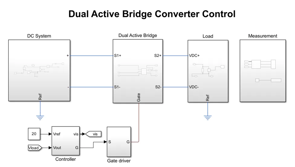
A complete dual active bridge control scheme is best understood as a closed loop wrapped around the converter. The block diagram above shows the functional pieces that every DAB control implementation shares, whatever modulation strategy runs underneath:
The closed loop is what makes the converter usable: the controller continuously adjusts the phase shift to hold the output at its setpoint as the source voltage, load current, and direction of power flow change. Everything covered above — SPS through TPS modulation, ZVS, and transient-DC-bias suppression — lives inside that controller-and-gate-driver path, which is exactly why it has to be verified in a real-time closed loop rather than on static waveforms alone.
A DAB is a nonlinear, time-varying system, which makes its control loop genuinely difficult to design well. The standard approach derives a small-signal averaged model of the converter—using reduced-order, generalized-state-space-averaging, or discrete-time methods—and then linearizes that model to tune the compensators. Discrete-time models tend to be favored at high switching frequencies because they better capture behavior within the ZVS interval, which an averaged continuous-time model can miss.
The typical structure is a cascaded outer-voltage / inner-current loop. Linear PI compensators are most common, but the literature also covers robust PI, sliding-mode control, feedforward-plus-feedback hybrids, disturbance-observer-based control, and model predictive control (MPC). MPC is prized for fast transient response but constrained by computational burden and sensitivity to model parameters—another reason platform compute capacity matters.
One failure mode deserves special attention: transient DC bias. When the phase shift between the bridges changes abruptly—during a load step, an output-voltage change, or a reversal of power-flow direction—a momentary imbalance in the volt-second product applied to the transformer can inject a DC offset into both the transformer’s magnetic flux and the inductor current. If left unmanaged, this can push the transformer core toward saturation, produce peak currents that exceed the safe ratings of the switches, cause oscillations on the DC bus voltage, and temporarily destroy the soft-switching condition the converter depends on for efficiency.
Suppressing this bias—through duty-cycle modulation, predictive flux balancing, double-sided SPS, soft-magnetizing soft-start, precise dead-time control, or dedicated current-injection windings—is essential for long-term reliability. It is also exactly the kind of fast, transient behavior that is extremely difficult to verify without testing the converter in a real-time closed loop, which is where dual active bridge simulation on hardware-in-the-loop platforms becomes indispensable.
The DAB earns its widespread adoption through a cluster of reinforcing advantages:
Selecting the optimal bidirectional DC-DC converter topology is a critical architectural decision that depends on voltage range, load profile, and power density requirements. The DAB and resonant topologies (LLC and CLLLC) are the leading candidates for high-power applications.
Architectural differences. The DAB uses a non-resonant inductive network where power transfer is governed by the phase-shift-induced voltage drop across a series inductor. LLC and CLLLC converters incorporate resonant tanks containing multiple reactive elements. An LLC converter uses a series resonant capacitor, a series resonant inductor, and a large magnetizing inductance. A CLLLC converter adds a matching resonant capacitor and inductor on the secondary side to achieve fully symmetrical bidirectional power flow.
Control paradigms. The DAB operates at a fixed switching frequency, regulating power and voltage by adjusting phase shift and duty cycle. This simplifies EMI filter design and magnetic core utilization. LLC and CLLLC converters typically rely on variable frequency modulation, sweeping the switching frequency across a wide range to navigate the gain curve of the resonant tank—which complicates magnetic optimization and can introduce unpredictable EMI behavior across the spectrum.
Soft-switching and loss profiles. For resonant converters, ZVS can be realized across all load conditions, including light loads and wide voltage ranges, and because the resonant current is sinusoidal, switches experience extremely low turn-off currents and minimal turn-off losses. In a DAB, switches experience high turn-off current under standard SPS, leading to higher turn-off losses across most of the voltage range. While the DAB can achieve full ZVS across its entire range using commutation inductors or advanced modulation, this can increase RMS current and conduction losses.
In short: choose the DAB for ease of bidirectional operation, modular high-power structures, and wide voltage ranges; choose LLC/CLLLC for fixed-ratio applications where light-load efficiency and low EMI dominate.
The performance ceiling of a modern DAB is set largely by its semiconductors. Silicon carbide (SiC) MOSFETs and gallium nitride (GaN) HEMTs enable switching frequencies from tens of kilohertz into the megahertz range, which shrinks the magnetics and pushes power density well beyond what silicon IGBTs allow. Peak efficiencies above 98 percent are well documented in SiC-based designs, with the highest-performing reference designs reporting peak efficiency near 99 percent.
The principal caveat is light-load behavior: when the phase shift is small, the inductor current may be insufficient for ZVS, and wide-bandgap devices that hard-switch can ring and dissipate. This is precisely why the modulation strategy and the device choice must be co-designed and co-validated—and why light-load operating points deserve dedicated test cases in any dual active bridge simulation campaign.
A DAB design is not proven until its control is proven, and offline simulation alone cannot prove implementation-level correctness. Dual active bridge simulation has to progress through clearly staged steps, ending in real-time, closed-loop validation.
Two properties make the DAB one of the most demanding converters to simulate in real time. First, it is operated at very high switching frequencies—commonly 100 kHz and rising into the hundreds of kilohertz—specifically to reduce the size and weight of the magnetics. Second, the fundamental harmonic of the transformer waveform equals the switching frequency, unlike grid-tied converters whose fundamental sits at 50 or 60 Hz. The DC-DC stage itself is therefore the hardest part of the converter to emulate accurately, because the simulator must resolve the carrier-level switching transitions, dead-time, and ZVS intervals that define the converter’s behavior—not a slow averaged envelope.
For DAB switching frequencies in the tens to hundreds of kilohertz, the real-time platform’s simulation time step should be at least twenty to a hundred times smaller than the switching period. For a 100 kHz converter, that points toward time steps on the order of 100 nanoseconds or smaller. A practical benchmark worth remembering: when PWM or phase-shift sampling error climbs above roughly one percent, the time step is too coarse to trust the ZVS and current-stress results. The difference is stark—a coarse step can produce sampling errors above twenty percent, while a sufficiently fine step holds error below one percent.
This requirement generally rules out CPU-only HIL platforms, which are typically capped near 50 kHz, and points toward FPGA-based emulation. A sequential CPU cannot deterministically resolve carrier-level PWM and fast switching transients at these frequencies, whereas an FPGA computes the circuit equations in parallel and delivers deterministic, nanosecond-scale steps. Switch-level oversampling is also necessary, because more than one gate transition can occur within a single simulation step in DAB applications; without it, numerical subharmonics and error appear.
A complete dual active bridge control validation program proceeds in stages:
Fault injection and power-reversal testing belong in this environment, not on a bench. Short circuits, voltage sags, grid faults, battery cell imbalance, and thermal-runaway scenarios can all be exercised safely and repeatably, with particular attention to charge-to-discharge transitions—exactly where transient DC bias and current overshoot tend to appear. Running these fault campaigns as a regression gate on every firmware build turns one-off testing into an ongoing safety net.
Finally, realistic sources and loads should be part of the test plan from day one. Replacing static bench supplies with emulated batteries and emulated grids exposes the DAB’s control loops to state-of-charge-dependent voltages, realistic impedance, and genuine disturbances—the actual conditions under which the converter has to remain stable in the field.
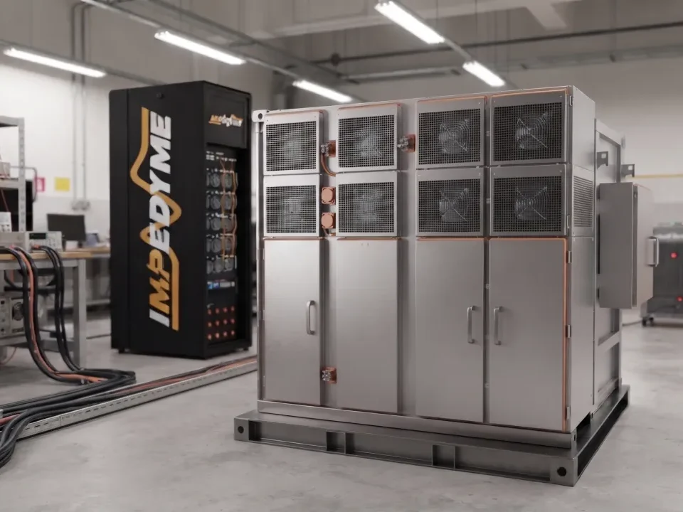
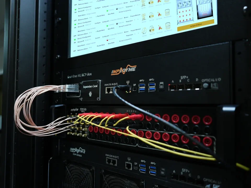
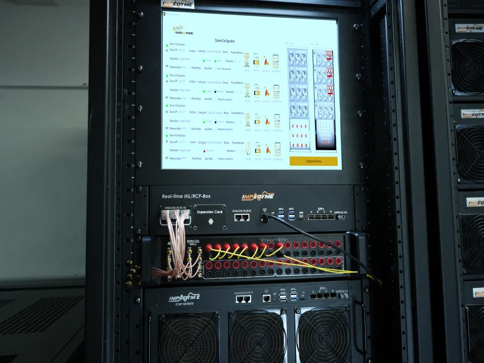
Impedyme’s FPGA-based real-time platform is built for exactly this class of fast-switching converter. With a 90 ns time step and AMD/Xilinx Zynq UltraScale+ processing, it resolves the carrier-level switching, dead-time, and ZVS behavior that coarser CPU-based systems average away. The full validation chain—controller HIL, power HIL, and rapid control prototyping—runs on one connected platform, so the same model an engineer tunes offline deploys to real-time hardware without rework.
In practice, this is what lets a team verify SPS, EPS, DPS, and TPS mode transitions, confirm ZVS coverage across the full voltage and load range, catch transient DC-bias events during power reversal, and prove protection logic against injected faults—all before the converter ever sees a live grid or a real battery pack.
The dashboard above shows what real-time dual active bridge control looks like from the operator’s seat on the Impedyme platform. From a single interface, an engineer sets the reference voltage and the PI controller gains (Kp and Ki) on the fly and immediately sees the effect: the output voltage tracking its setpoint, the load current and power settling, and the grid-side voltage and current responding in real time. There is no recompile-and-rerun cycle—gains are tuned against live hardware behavior.
Two things make this more than a visualization. First, the protection layer—over-current, over-temperature, and over-voltage flags with a converter on/off control—runs in the loop, so fault response can be exercised safely rather than assumed. Second, every quantity that matters for dual active bridge control is observable at once: reference tracking, load power, and grid current are all on screen together, which is exactly what it takes to confirm ZVS coverage, catch transient DC-bias events, and validate mode transitions before the converter is connected to a real source or load.
Choosing a modulation scheme should follow directly from the operating envelope. If a design runs near a unity voltage ratio at fairly steady load, SPS may be adequate. Any application spanning a wide voltage range or significant light-load operation—EV charging, battery storage—should budget from the outset for EPS, DPS, or TPS, treating the resulting mode transitions as test cases in their own right. A useful trigger for escalating to a more sophisticated scheme is whenever light-load efficiency or ZVS coverage falls short of target across the required voltage range.
Validation should proceed in staged steps: offline modeling for design and gain tuning, then deployment of that same model to FPGA-based real-time hardware for controller HIL testing of firmware and timing, and only then power HIL testing for full-power closed-loop verification. Offline simulation alone should never be treated as sufficient evidence of implementation-level correctness.
Fault injection and power-reversal testing should be mandatory, not optional, with particular attention to charge-to-discharge transitions. And time-step adequacy deserves explicit scrutiny rather than being taken on faith: for switching frequencies in the tens to hundreds of kilohertz, an FPGA-based platform with a sufficiently fine time step is the only way to trust ZVS and current-stress results.
What is dual active bridge control?
Dual active bridge control regulates power and voltage by commanding the phase shift between the two bridges’ square-wave voltages. The phase difference sets a voltage across the series inductor that drives current and transfers power; the direction and magnitude of power depend on the sign and size of that phase shift.
At what phase shift is power transfer maximized?
Maximum active power transfer occurs at a normalized phase shift of one-half, corresponding to a ninety-degree phase displacement between the primary and secondary square waves. Operating beyond ninety degrees is avoided because power sensitivity reverses and circulating currents grow.
What causes transient DC bias and how is it prevented?
Abrupt phase-shift changes—during load steps or power-flow reversal—can create a volt-second imbalance that injects a DC offset into the transformer flux and inductor current, risking core saturation and overcurrent. It is mitigated through duty-cycle modulation, predictive flux balancing, double-sided SPS, soft-start, and precise dead-time control.
What is the difference between HIL and PHIL for dual active bridge validation?
Controller HIL tests the real controller against a signal-level emulated converter to verify firmware, timing, and protection logic. Power HIL exchanges real power through an amplifier with emulated sources and loads to verify full-power, closed-loop behavior. HIL pulls software bugs forward; PHIL pulls power-stage issues forward.
What efficiency can a dual active bridge achieve?
With proper design and wide-bandgap devices, well-designed DAB converters reach peak efficiencies above 98 percent, with the best SiC and GaN designs approaching 99 percent. Efficiency is highest near a matched voltage ratio and degrades at light load or large voltage mismatch under simple SPS control.