
Full bridge rectifier is the arrangement of four diodes that turns alternating current into direct current by using both halves of the AC cycle, and it sits at the input of almost every mains-fed converter built today. Engineers reach for the full bridge rectifier rather than a simpler single-diode circuit for three practical reasons: it wastes none of the input waveform, it produces ripple at twice the supply frequency so the filter that follows can be smaller, and it needs no centre-tapped transformer. Those three advantages are why full bridge rectifiers appear in EV chargers, motor drives, switch-mode power supplies, and industrial DC buses, while the half-wave alternative has been pushed to the margins. This guide covers what the circuit is, how it works cycle by cycle, how to size the components, where full bridge rectification shows up in modern power electronics, and how a rectifier front end is validated once it exists in hardware.
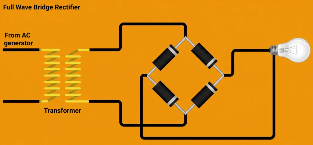
A full bridge rectifier is a full bridge rectifier circuit built from four diodes connected in a closed loop, with the AC source applied across one pair of opposite corners and the load taken from the other pair. The arrangement is often drawn as a diamond, which is why the term full bridge diode configuration is used interchangeably with diode bridge. Whatever the drawing convention, the electrical behaviour is the same: whichever way the input polarity swings, two of the four diodes are forward biased and steer current through the load in a single, unchanging direction.
That steering action is the whole point. The input alternates; the load current does not. The result at the output is a series of positive humps, one for each half of the input cycle, rather than the positive-and-negative swing that went in. This is what distinguishes full bridge rectification from half-wave rectification, where the negative half of the cycle is simply discarded and the output sits at zero for half the time.
The same topology is sold as discrete diodes and as a single four-terminal package. A packaged part carrying the label full diode bridge rectifier contains exactly the circuit described above, pre-assembled with two AC input terminals and two DC output terminals, and is frequently the cheaper and more thermally predictable option. Larger power designs still use discrete diodes so that each device can be heatsinked and specified independently.
The operation of a full bridge rectifier depends on one property of the diode: it conducts readily in one direction and blocks in the other. Arrange four of them correctly and the conduction path reverses in step with the input, while the direction of current in the load stays fixed.
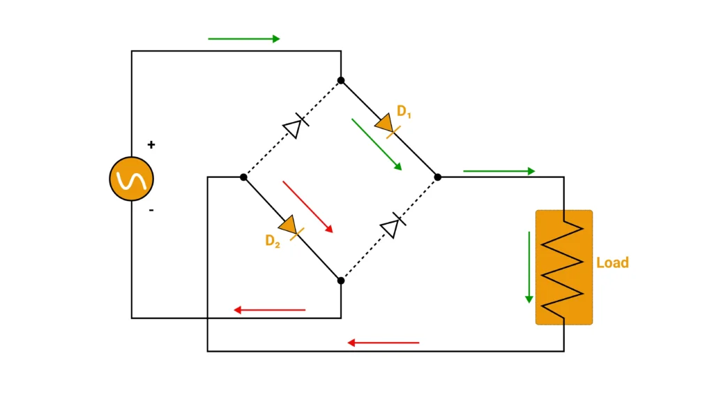
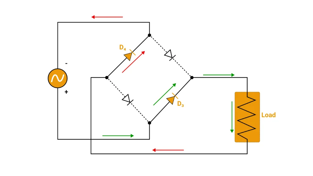
At any instant, one input terminal of the bridge is more positive than the other. Current leaves that terminal, finds the one diode oriented to let it through toward the positive output rail, passes through the load, returns to the negative output rail, and finds the one diode oriented to let it back to the other input terminal. The remaining two diodes are reverse biased and behave as open circuits for that half of the cycle. When the input polarity flips, the roles swap: the previously blocking pair conducts, the previously conducting pair blocks, and — critically — the direction of current through the load is unchanged.
Two consequences follow immediately from this, and both matter in design.
First, two diodes are always in series with the load. The forward voltage of each one is subtracted from the delivered output, so a silicon full bridge rectifier typically loses somewhere around one and a half volts across the pair at moderate currents. That loss is trivial on a 400-volt bus and severe on a 5-volt output.
Second, because both halves of the input are used, the output ripple appears at twice the supply frequency. On a 50 Hz supply the ripple sits at 100 Hz, and on a 60 Hz supply at 120 Hz. Higher-frequency ripple is easier and cheaper to filter, which is one of the strongest arguments for full bridge rectification over the half-wave alternative.
The term full wave bridge rectifier describes the same circuit from the perspective of the waveform rather than the topology. “Full wave” means the rectifier acts on the entire input waveform, both the positive excursion and the negative one, rather than on half of it. Following the current through each half of the cycle in turn is the clearest way to understand why the four-diode arrangement behaves as it does, and it is worth doing carefully because this is where most explanations of the full bridge rectifier circuit get skimmed.
During the positive half-cycle, the upper input terminal of the bridge is positive with respect to the lower one. Two diodes on opposite sides of the bridge become forward biased and conduct — in the conventional labelling, D1 and D2. Current flows out of the source, through the first conducting diode, down through the load from top to bottom, back through the second conducting diode, and returns to the source. The other two diodes see reverse voltage across them and block.
Half a cycle later the source polarity reverses and the lower input terminal becomes the positive one. The pair that was blocking — D3 and D4 — now conducts, and the pair that was conducting now blocks. The path through the bridge is completely different, but the path through the load is identical: current still enters at the top of the load and leaves at the bottom.
That is the entire trick of the full bridge rectifier. The conduction path alternates; the load current does not.
With nothing but a resistive load connected, the output of a full bridge rectifier is a train of positive half-sine humps butted against one another with no gaps. Every negative excursion of the input has been folded upward into a positive one, so the waveform touches zero twice per input cycle but never goes below it.
This waveform is direct current only in the loose sense that its polarity never reverses. Its instantaneous value swings from zero to the peak and back again, twice per input cycle, which no practical load will tolerate as a supply rail. The average value of this unfiltered waveform sits at roughly nine-tenths of the RMS input voltage for an ideal bridge, less the two diode drops in the conduction path — a useful figure to carry around, because it tells you immediately that a transformer secondary must be specified above the target DC output rather than at it.
The gap between this waveform and a usable DC rail is what the rest of the power supply exists to close. A smoothing capacitor is the first and most common step, and it changes the behaviour of the full bridge rectifier considerably more than most descriptions admit.
There is no difference. A full bridge rectifier and a full wave bridge rectifier are the same circuit under two names — one naming the topology, the other naming the waveform behaviour. Search results treat them as distinct because both phrases are in common use, but any part sold under either name is the same four-diode arrangement.
The genuine distinction worth drawing is between the bridge and the centre-tapped full-wave rectifier, which also rectifies both halves of the cycle but does so with only two diodes and a transformer whose secondary is tapped at its midpoint. Both are full-wave circuits. Only one of them is a bridge.
The trade between them is straightforward. The centre-tapped circuit puts only one diode drop in the conduction path, which is attractive at low output voltages, but it demands a special transformer, uses only half the secondary winding at a time, and exposes each diode to roughly twice the reverse voltage. The bridge needs four diodes and pays two forward drops, but works from any ordinary secondary — or directly from the mains with no transformer at all.
Table 1 — Rectifier topologies compared
| Half-wave | Centre-tapped full-wave | Full bridge rectifier | |
|---|---|---|---|
| Number of diodes | 1 | 2 | 4 |
| Transformer requirement | Ordinary secondary | Centre-tapped secondary | Ordinary secondary, or none |
| Input cycle used | One half only | Both halves | Both halves |
| Output ripple frequency | Equal to supply frequency | Twice supply frequency | Twice supply frequency |
| Diode drops in the load path | One | One | Two |
| Reverse voltage per diode | Peak input | Roughly twice peak half-secondary | Approximately peak input |
| Transformer utilisation | Poor | Moderate — half the winding at a time | Good |
| Filtering effort required | High | Moderate | Moderate |
| Typical application | Trickle chargers, signal detection | Legacy low-voltage supplies | General AC-DC front ends |
Adding a capacitor across the output of a full wave bridge rectifier transforms the humped waveform into something close to a DC rail. The capacitor charges toward the peak of each hump and then supplies the load from stored energy while the rectified waveform falls away, so the output no longer returns to zero. What remains is a sawtooth ripple riding on a mostly steady voltage.
The behaviour is easy to state and easy to under-appreciate. Larger capacitance means less ripple. It also means the capacitor spends less of each half-cycle charging, because it only draws current during the brief window when the rectified waveform exceeds the voltage already stored. That window — the conduction angle — narrows as capacitance grows, and since the same average charge must be replaced in a shorter time, the peak current through the diodes rises sharply.
This is the single most consequential fact about a capacitor-input full bridge rectifier, and it drives three design decisions at once. The diodes must be rated for repetitive peak current, not merely for the average DC output current. The capacitor must be rated for the ripple current flowing in and out of it every half-cycle, which is what determines its heating and its service life. And the transformer or supply feeding the bridge sees a distorted, pulsed current draw rather than a clean sinusoid.
Power-up brings a separate problem. At the instant the supply is applied, the capacitor is empty and looks like a short circuit, so inrush current is limited only by the source impedance and the wiring. Two mitigations are standard: a negative temperature coefficient thermistor in series, which is resistive when cold and drops away as it heats, or a resistor bypassed by a relay or thyristor that closes once the capacitor has pre-charged. Larger systems favour the second because the thermistor’s protection fades if the equipment is power-cycled quickly.
Where ripple must be lower still, an inductor placed before the capacitor forms an LC filter that both reduces ripple and widens the conduction angle, easing the peak-current demand on the full bridge diode set at the cost of size and weight.
Five characteristics govern how a full bridge rectifier behaves in a real design.
Average DC output. With a resistive load and no filtering, the average output sits at approximately nine-tenths of the RMS input, minus the two diode drops. Add a smoothing capacitor and the output rises toward the peak of the input instead, again less the two drops, because the capacitor holds near the crest. The distinction matters when specifying a transformer: the same secondary produces noticeably different DC rails depending on whether the filter is present.
Ripple frequency. Twice the supply frequency, always. This is the direct consequence of using both halves of the cycle, and it is a genuine advantage — the filter components see a ripple frequency they can attenuate more easily than the line frequency ripple a half-wave circuit produces, so both the capacitor and any inductor can be smaller for the same result.
Forward voltage loss. Two diodes conduct at all times, so the loss is twice the forward drop of one device, multiplied by the load current. Standard silicon rectifier diodes are the most expensive in this respect. Schottky devices roughly halve the drop, which is significant on a low-voltage output and largely irrelevant on a high-voltage one.
Peak inverse voltage. Each non-conducting diode must withstand approximately the peak input voltage in reverse. Practice is to specify devices well above that figure, because mains supplies carry transients and surges that briefly exceed the nominal peak by a wide margin. A margin of two times the calculated peak is common, and more where the supply is known to be electrically noisy.
Efficiency. Losses in a full bridge rectifier come almost entirely from conduction in the two active diodes, with a smaller contribution from reverse recovery when fast-switching devices are not used and from leakage in the blocking pair. At high output voltage the efficiency of a diode bridge is excellent. At low output voltage the fixed forward drops dominate, and the case for active rectification opens up.
Table 2 — Characteristics at a glance
| Parameter | Behaviour in a full bridge rectifier | Design implication |
|---|---|---|
| Average DC output (unfiltered) | About nine-tenths of RMS input, less two diode drops | Specify the secondary above the target rail |
| Average DC output (capacitor filtered) | Approaches input peak, less two diode drops | Higher rail than the unfiltered case from the same winding |
| Ripple frequency | Twice supply frequency | Smaller filter components for a given ripple target |
| Conduction path | Two diodes in series at all times | Doubled forward loss versus centre-tapped |
| Peak diode current | Far above average output current with capacitor input | Rate diodes on repetitive peak, not average |
| Peak inverse voltage | Approximately the input peak | Specify with substantial voltage margin |
| Inrush at power-up | Limited only by source and wiring impedance | Requires NTC or pre-charge circuit |
| Input current shape | Short, tall pulses when capacitor filtered | Drives harmonic distortion; usually needs PFC |
Choosing the parts for a full bridge rectifier comes down to matching the diode family to the application, then rating the devices for the conditions they will actually see rather than the nominal ones.
Standard recovery diodes are the default for line-frequency rectification. They are inexpensive and robust, and their slow reverse recovery is irrelevant at 50 or 60 Hz. Fast recovery diodes are used where the bridge sees higher-frequency switching or where reverse recovery current would generate unacceptable noise. Schottky diodes offer a much lower forward drop and negligible recovery charge, but have limited reverse voltage ratings and higher leakage that worsens with temperature, restricting them mostly to low-voltage outputs. Silicon carbide Schottky diodes lift that voltage restriction and effectively eliminate recovery losses, at a price premium that high-power and high-efficiency designs increasingly accept.
The choice between discrete diodes and a packaged bridge is largely thermal and mechanical. A packaged full diode bridge rectifier is compact, cheap, and simple to mount, but concentrates all four devices’ losses into one thermal path. Discrete diodes spread the heat, allow individual heatsinking, and give freedom to mix device types, at the cost of board area and assembly complexity.
Ratings deserve care. Average forward current is the least useful number on the datasheet for a capacitor-input design, because the repetitive peak current is several times higher. Non-repetitive surge current rating governs survival of the first power-on inrush. Reverse voltage should carry the margin described earlier. And all of these ratings degrade with junction temperature, so derating curves must be read at the temperature the device will actually reach, not at the 25 °C headline condition.
Table 3 — Diode family selection for a full bridge rectifier
| Diode family | Forward drop | Reverse voltage capability | Best suited to |
|---|---|---|---|
| Standard recovery silicon | Highest | High | Line-frequency mains rectification |
| Fast recovery silicon | High | High | Higher-frequency or noise-sensitive designs |
| Schottky | Lowest | Limited | Low-voltage, high-current outputs |
| Silicon carbide Schottky | Low | High | High-voltage, high-efficiency front ends |
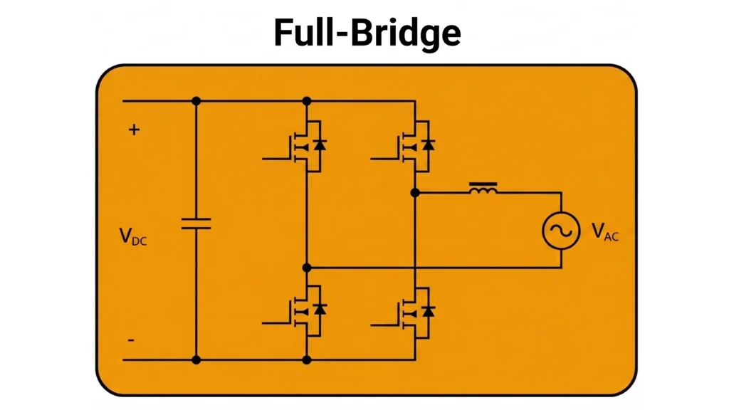
The fixed forward drop of a diode is a floor on efficiency that no amount of thermal design removes. An active full bridge rectifier breaks through that floor by replacing the diodes with MOSFETs and switching them deliberately in synchronism with the input. Because a MOSFET behaves as a resistance when it is on, the conduction loss falls with the device’s on-resistance rather than sitting at a fixed voltage. Paralleling devices or choosing lower-resistance parts buys efficiency directly, which is impossible with a diode.
Two implementations are common. Dedicated ideal-diode-bridge controllers sense the input polarity and drive the MOSFET gates automatically, presenting the same two-terminal-in, two-terminal-out interface as a conventional bridge and dropping into existing designs with little redesign. Fully controlled active front ends go further, using the same four-switch structure to shape the input current and regulate the DC bus, which is how large drives and chargers achieve near-unity power factor without a separate stage.
Synchronous rectification introduces failure modes that diodes do not have. If both devices in one leg conduct simultaneously — even briefly — the result is a shoot-through short across the source. Gate timing must therefore include dead time, an interval where both devices are off. During that interval the MOSFET body diode carries the current, and because body diodes generally have poor forward and recovery characteristics, excessive dead time gives back much of the efficiency the topology was adopted to gain. Tuning that interval is the central design problem of full bridge rectification with active devices.
The added complexity pays where the fixed diode drop is a large fraction of the output: low-voltage rails, high output currents, thermally constrained enclosures, and battery-powered equipment where every fraction of a percent of efficiency extends runtime. On a high-voltage DC bus, a diode bridge usually remains the sensible answer.
Four is the minimum number of diodes that can route both polarities of an input to a single-polarity output without help from a transformer tap. Two of them form the path that conducts on the positive half-cycle; the other two form the path that conducts on the negative half-cycle. Remove any one and the bridge loses its ability to handle one polarity, collapsing into half-wave behaviour.
The alternative that uses fewer devices — the centre-tapped circuit — buys that reduction with a specially wound transformer and with diodes that must block roughly twice the reverse voltage. In other words, the fourth diode in a full bridge rectifier is not redundancy. It is what removes the transformer requirement entirely, which is precisely why the bridge can be connected straight across the mains in equipment that has no transformer at all.
Selecting among full bridge rectifiers for a given design is a matter of working through five questions in order.
Start with the reverse voltage the devices will see, take the peak of the highest expected input, and apply generous margin for transients. Then establish the current profile: not just the average DC output current, but the repetitive peak current the capacitor-input filter will demand and the one-off surge at power-up. Third, decide how much the forward drop costs you — on a low-voltage rail it may justify Schottky devices or an active bridge, and on a high-voltage rail it will not.
Fourth, work out the thermal path before choosing a package. Total dissipation is the forward drop multiplied by the current, doubled for the two conducting devices, and it must leave the package and reach ambient through whatever heatsinking the enclosure allows. A packaged bridge that is electrically adequate will still fail if the thermal design assumes free air that the enclosure does not provide.
Finally, consider the operating environment: ambient temperature, altitude, supply quality, vibration, and whether the equipment will be power-cycled frequently. Frequent cycling in particular undermines NTC-based inrush limiting and pushes the design toward an active pre-charge arrangement.
The full bridge rectifier is not a legacy circuit kept alive by textbooks. It is the front end of most equipment that draws power from an AC supply.
In EV charging, both onboard chargers and off-board DC fast chargers begin by rectifying the incoming AC to establish a DC link, which downstream converters then shape into the voltage and current the battery requires. Three-phase versions of the same bridge do this job in higher-power charging equipment. In motor drives, the input stage rectifies the supply to a DC bus from which the inverter synthesises variable-frequency output — the rectifier defines the bus the entire drive works from. In switch-mode power supplies, the bridge sits directly across the mains ahead of a power factor correction boost stage, which is why so much attention is paid to the current waveform it draws.
Aerospace and marine power conversion uses rectifier front ends to bring generator output into a DC distribution system, often at frequencies well above 50 or 60 Hz. Renewable and storage converters use them wherever an AC source or grid connection must feed a DC bus. And in a quite different role, a full bridge diode arrangement is used for reverse-polarity protection, passing supply current regardless of which way round the input is connected — a common feature in industrial and automotive equipment where field wiring cannot be guaranteed.
A capacitor-input full bridge rectifier draws current only during the short window each half-cycle when the input exceeds the stored voltage. The result is a series of short, tall current pulses rather than a sinusoid that follows the voltage.
This has consequences beyond the equipment itself. The pulsed current is rich in harmonics, and while the fundamental component may be almost in phase with the voltage, the distortion still degrades the true power factor substantially. A rectifier front end can therefore appear well behaved by one measure and poor by another — displacement power factor near unity, distortion power factor far from it. Multiply that across many units on the same supply and the harmonic currents add up, distorting the voltage waveform for everything else connected nearby.
This is why an active power factor correction stage almost always follows the bridge in modern mains equipment. The PFC stage forces the input current to track the voltage waveform, converting the pulsed draw into something close to sinusoidal. It is also why grid-connected equipment is subject to harmonic emission limits in most markets, and why the input current waveform of a rectifier design has to be measured rather than assumed.
Most full bridge rectifier failures announce themselves clearly once you know what to look for.
A shorted diode places a direct path across the supply on alternate half-cycles. It usually takes the input fuse with it, and if the fuse survives, the transformer or supply sees heavy current and heats rapidly. An open diode is quieter and more insidious: the bridge continues to work, but only on one polarity. The symptom is a halved output with much larger ripple, and — diagnostically decisive — ripple at the supply frequency rather than at twice it.
Thermal failure follows undersized heatsinking or an enclosure that runs hotter than the design assumed. Leakage rises with junction temperature, which raises dissipation, which raises temperature further, so the failure tends to accelerate. Capacitor ageing presents as slowly increasing ripple over months or years as equivalent series resistance climbs and capacitance falls; the diodes are innocent, but they suffer the higher peak currents that result. Surge damage from lightning or switching transients typically appears as a shorted device with visible package damage.
Diagnosis is straightforward with three techniques. A multimeter in diode-check mode, with the bridge disconnected, identifies shorted and open devices directly. Ripple measured at full load, with attention to its frequency as well as its amplitude, distinguishes a lost diode from a tired capacitor. And thermal imaging under load finds the device that is running hot before it fails, which is far more useful than finding it afterwards.
A full bridge rectifier is easy to model and easy to build. The failures show up in the interaction between the two — between the rectifier, the source feeding it, and the converter drawing from it. That interaction is where we focus, and it is where most validation programmes are thinnest.
Five measurements separate a rectifier front end that works on the bench from one that works in the field. Ripple must be measured at full load rather than no load, and its frequency checked as well as its magnitude. Thermal rise must be recorded at rated current in the actual enclosure, not in free air. Inrush must be captured at cold start, and repeated after a short power interruption, because that is the condition that defeats thermistor-based limiting. Input current waveform and distortion must be measured, not inferred from the DC output. And behaviour must be confirmed at the extremes of the supply range, including undervoltage conditions where conduction angles widen and peak currents shift.
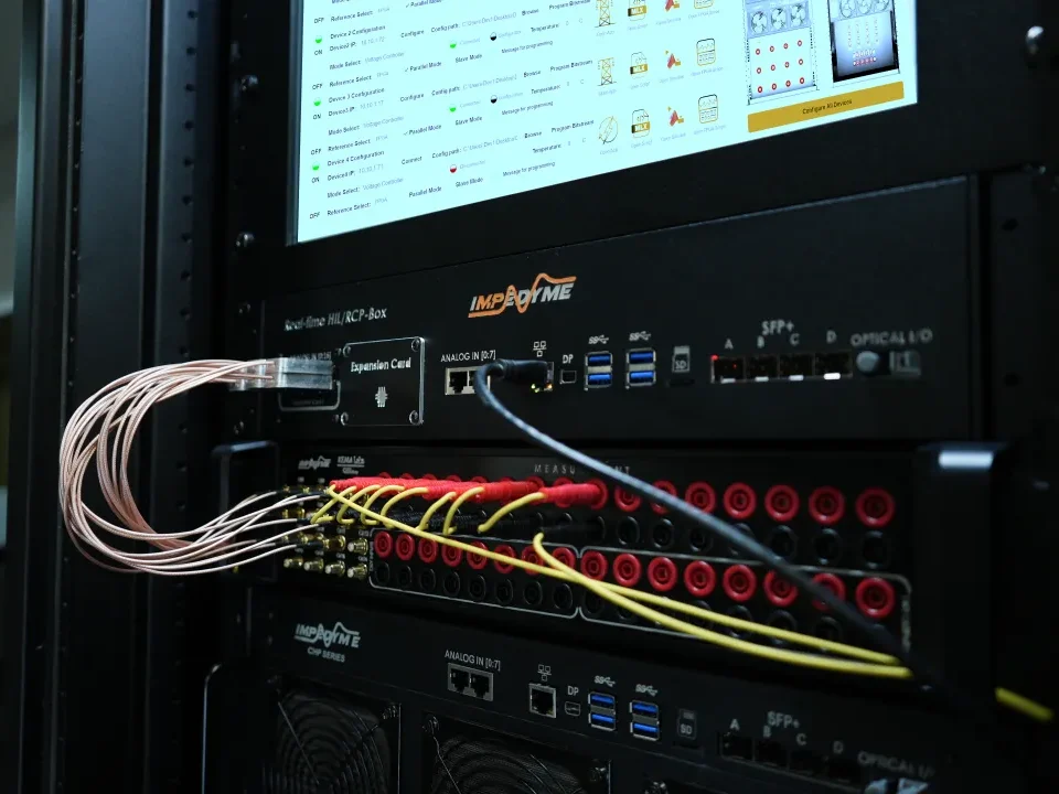
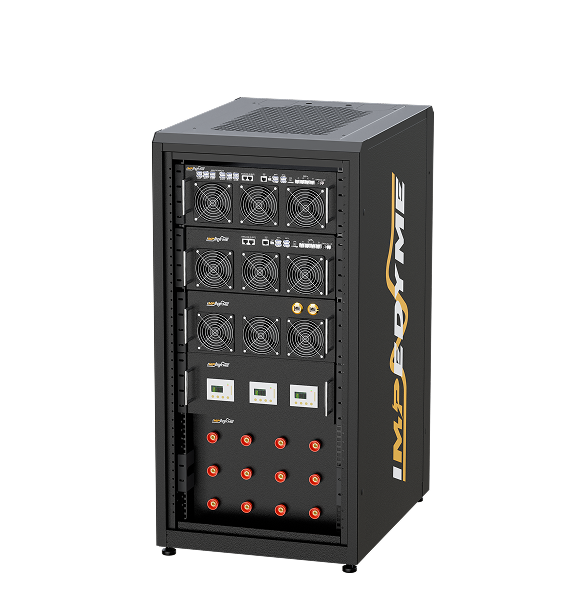
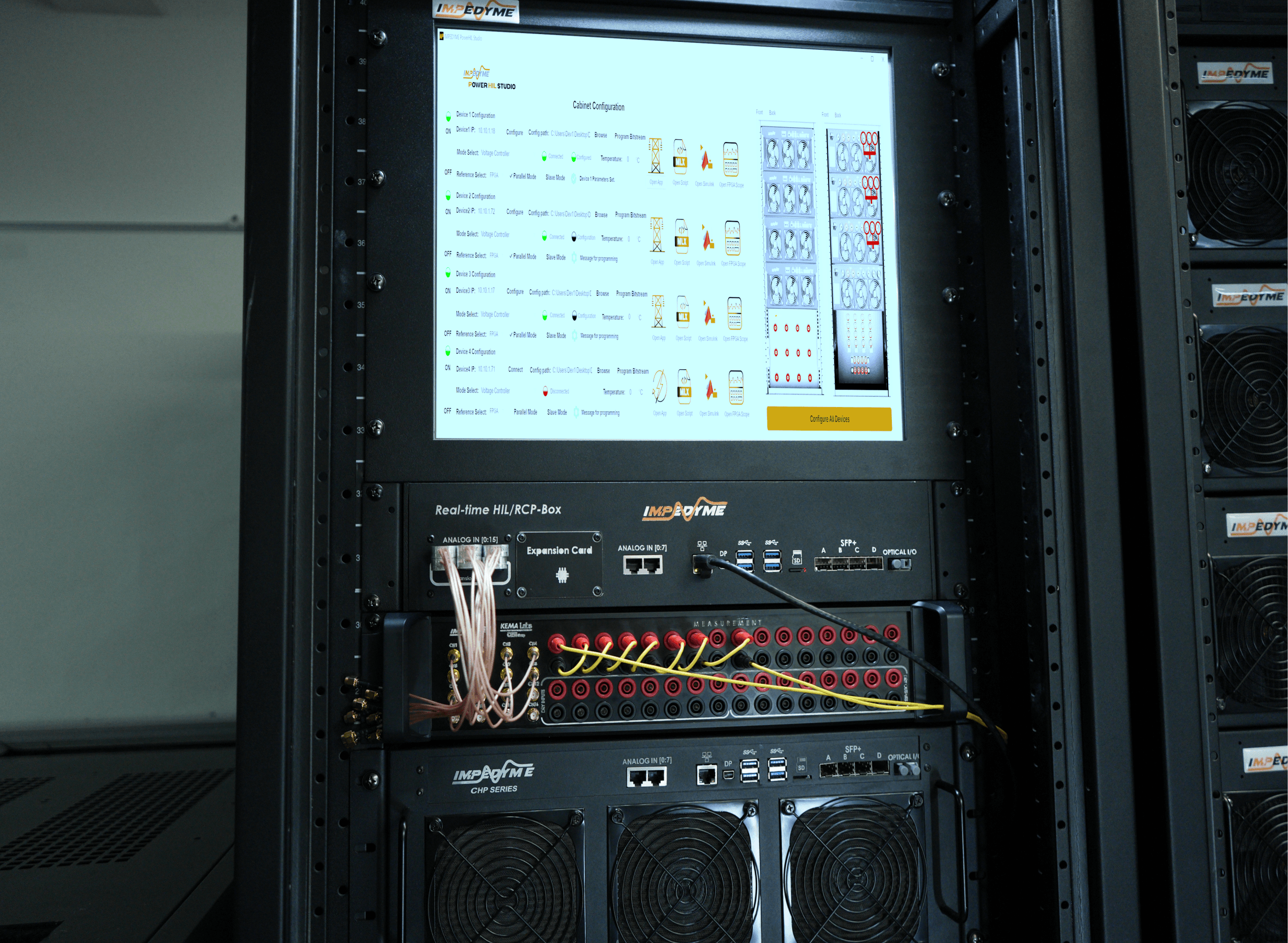
Offline simulation handles the ideal rectifier well and the interesting cases poorly. It struggles with the timing detail of narrow conduction windows, with the interaction between rectifier and downstream control loops, and with anything involving a real controller reacting to a real disturbance. Real-time simulation closes that gap by running models of the source, the rectifier stage, and the downstream converter fast enough to exchange signals with physical hardware as it operates. With PowerHIL Studio running on the CHP Series platform, we model the rectifier front end and the system around it at the timestep the switching behaviour actually demands, so control interactions appear in the test rather than in the field.
Power hardware-in-the-loop goes further by placing the real rectifier hardware between an grid emulator and an emulated load. Using GridSim Studio, we present the rectifier with sags, swells, phase loss, frequency deviation, distorted and unbalanced supplies, and fault conditions that would be unsafe, destructive, or simply impractical to create on a bench with a real supply. The DC side can be loaded with an emulated converter or battery rather than a resistor bank, so the rectifier sees the pulsed, dynamic loading it will meet in service. Every one of these conditions is repeatable on demand, which turns rectifier validation from a sampling exercise into a systematic one.
The full bridge rectifier endures because its four-diode arrangement solves the AC-to-DC problem with no transformer tap, no wasted half-cycle, and ripple at a frequency that is comparatively easy to filter. Understanding it properly means going past the full bridge rectifier diagram to the consequences that follow from it: two forward drops in the conduction path, peak diode currents far above the average output current once a smoothing capacitor is fitted, a distorted input current that usually needs a power factor correction stage behind it, and a thermal design that governs whether the circuit survives.
The direction of travel is toward active devices and controlled front ends. Synchronous full bridge rectification with MOSFETs removes the fixed diode drop where efficiency justifies the complexity, and fully controlled front ends fold rectification and power factor correction into one stage. Both raise the validation burden considerably, because the failures move from the components into the control interactions between them. Testing a rectifier front end against a real grid and a real load — including the disturbances it will only meet once in service — is what closes that gap.
How much voltage is lost across a full bridge rectifier?
Two diodes conduct at all times, so the loss is roughly twice the forward drop of a single device — about one and a half volts for standard silicon at moderate current. Schottky devices roughly halve this, which matters on low-voltage outputs and very little on high-voltage ones.
What is the ripple frequency at the output of a full bridge rectifier?
Twice the supply frequency, because both halves of the input cycle are used. That means 100 Hz on a 50 Hz supply and 120 Hz on a 60 Hz supply. Higher ripple frequency allows smaller filter components for the same ripple target.
Why does a full bridge rectifier draw such high peak currents?
With a smoothing capacitor fitted, the diodes conduct only during the brief window when the rectified waveform exceeds the stored capacitor voltage. The same average charge must be replaced in that short window, so peak current runs several times higher than the average output current.
What is an active or synchronous full bridge rectifier?
An active full bridge rectifier replaces the diodes with MOSFETs switched in synchronism with the input. Conduction loss then depends on device on-resistance rather than a fixed voltage drop, improving efficiency substantially on low-voltage, high-current outputs at the cost of gate timing complexity.
How do you test a full bridge rectifier?
Check individual devices with a multimeter in diode-check mode to find shorted or open diodes. Measure ripple amplitude and frequency at full load — ripple at the supply frequency rather than twice it indicates a lost diode. Thermal imaging under load identifies devices running hot before they fail.